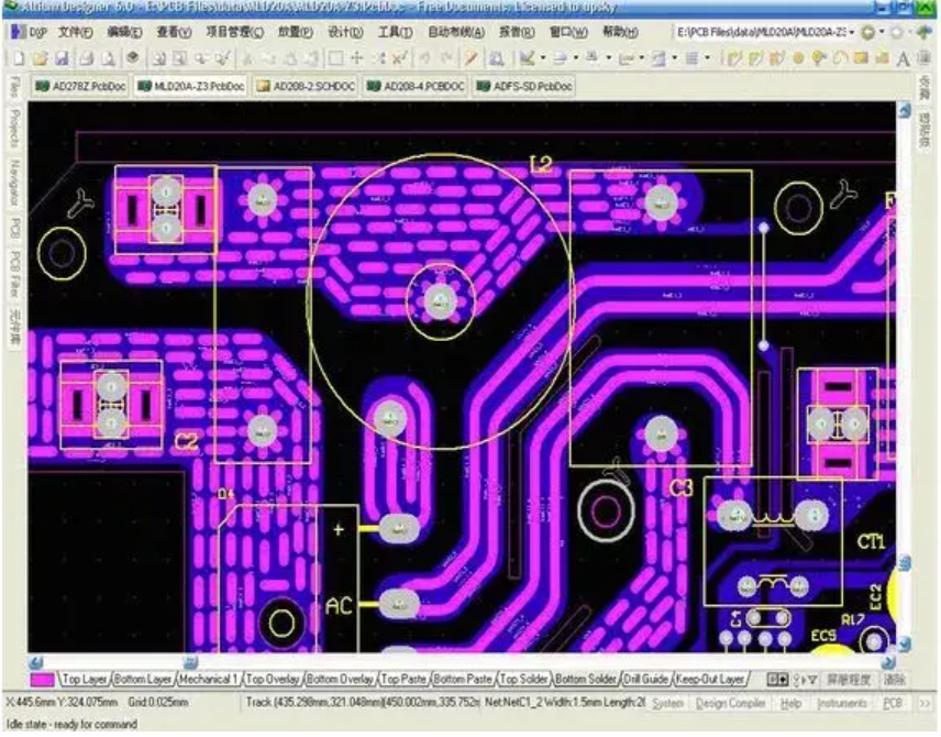

Recently, I have been making some modifications to the demo board based on the original chip factory.
What is the difference between our development model and when we were at Huawei?
In the original design, some wiring was intentionally insulated between signals through GND copper coating in the middle.
This reminds me of an article by Jiang Xiuguo, which explains "Is it a question whether to protect the ground wire or not when designing high-speed PCBs?"
We have also published articles about "crosstalk".
There are many methods to reduce crosstalk, including the sources and formation of crosstalk, the types of crosstalk, simulation and testing of crosstalk, etc. Among them, one method to reduce crosstalk is "ground wire isolation", which is to protect important signal networks and land networks. During the PCB design process, the added ground network is called the protection line, as shown in the following figure:
Can this local network really protect the signal network? Especially for the type of ground network shown in the above figure (without ground via).
Often in the design process, we are conflicted:
1. Is the addition of this GND network effective?
2. How much width does this GND network increase effectively?
3. How many via holes do we need to drill for this GND network?
Normally, if there is no design of a protective zone or the structure of an isolation zone is shown in the following figure:
For such complex problems, we can conduct simulation analysis through modeling. By establishing a simple model in ADS, qualitative research can be conducted on it. Different structures can be modeled as follows.
When considering a protected area, the general protective ground wire will be 1W (line width) away from the protected signal network, or greater than a 1W, as shown in the figure.
Simulation 1: We set up a protective ground with a width of 1w and ensure good grounding
The modeling is shown in the following figure:
The simulation results of near end and far end crosstalk are shown in the following figure:
Simulation 2: We set up a protective ground with a width of 1w and arrange 1/10 wavelength through holes for grounding
If the protective ground is grounded at one tenth wavelength (equivalent to grounding via), its structure is shown in the following figure:
The simulation results of near end and far end crosstalk are shown in the following figure:
Simulation 3: We will suspend the copper covering with a width of 1w, without grounding
Its structure is shown in the following figure:
The simulation results of near end and far end crosstalk are shown in the following figure:
Simulation 4: No protective ground, but increasing signal spacing
The distance between the two signal networks will be relatively large, and the modeling is shown in the following figure:
The simulation results of near end and far end crosstalk are shown in the following figure:
Four simulation conclusions are put together, and the conclusions are clear at a glance:
Sky blue (worst) dB (Guardtrace_open.. S (3,1)) with copper coating and no grounding (open circuit)
Blue (poor) dB (Guardtrace_2.. S (3,1)) has a protective ground, but no through-hole
Red (better): dB (S (3,1)) without protective ground wire, increasing spacing
Purple (optimal) dB (Guardtrace_2gnd.. S (3,1)) results with protected ground, with 1/10 wavelength ground hole
From the comparison results, it is evident that when a protective ground is added but not connected to GND, crosstalk is the largest (blue), and the suspended copper coating in the middle not only fails to provide isolation, but also increases the propagation path of crosstalk.
When a protective ground is added, but if a ground hole is not added according to one tenth of the wavelength, crosstalk will also be relatively large. Although the ground wire can provide isolation, it does not have enough knowledge of impedance and is not well grounded, which cannot provide good protection.
If there is enough space without protection, the result is relatively good, but it will be larger than adding a ground hole at one tenth of the wavelength. This depends on the size of the spacing, and a sufficiently large spacing often does not meet the conditions. A sufficiently large spatial distance can certainly reduce the spatial coupling of signals, but high-density PCB designs often cannot achieve this.
We have set up protective areas and installed protective holes at intervals of less than 1/10 wavelength, which can effectively suppress crosstalk. We need to focus on high-speed signals and effectively control crosstalk through protective measures.
The above conclusions are often not obtained through actual measurement, as they require a large number of testing instruments and a sufficient number of test PCBs, which requires a significant amount of cost. If we have simulation tools, they will become our design tools.